ST Nucleo 64 F401RE NF
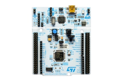
The board used in this community contribution is the NUCLEO64_F401RE board from ST. The board can be purchased from various sources and should be about 20 euros. Further information on the Nucleo64 boards can be found in the user manual UM1724 over at the ST website. The board used here is of revision c as can be found on the board's lower backside sticker. The board MB1136 C-02 is configured to use ST-LINK MCO as clock input for HSE so we have an HSE of 8 MHz. Plus X2 is mounted so we do have an LSE as well. This is reflected in the mcuconf.h in both nanoBooter and nanoCLR paths. If it is chosen to activate LSE as this is a for more accurate clock for RTC, the board.h file needs to be adjusted accordingly to use 32768 frequency for LSE.
I prepared a custom made a 4-wire jumper to USB cable by cutting off one end (Type A part) and figuring out the required D+, D-, 5V and GND. These need to be connected as follows:
USB V5 -> Can be ignored USB GND -> GND on CN7 USB D- -> PA11 on CN10 (outer row 7th pin from top) USB D+ -> PA12 on CN10 (outer row 6th pin from top)
Once these are connected and nanoFramework is flashed using the STM32 ST-LINK Utility the device should be visible in the Printf via SWO viewer function in the ST-LINK utility. Please set the frequency to match to what has been set in mcuconf.h (for the STM32F401RE it is 84MHz) and the Stimulus port to 0 and than hit start. If the board doesn't show then a reset (Black button on board) should do it.
We can now fire up Visual Studio and view the Device explorer window the board should be visible there as well. Select the board (if not done already) and hit the device capabilities button. The board specifics can than be seen in the output window.
Now you can start your adventure in the nanoFramework world and use one of the samples and adjust to the board specific features. Try to make a sample of yourself and publish it, for example, on Hackster.IO to show your achievement.
For your convenience I've listed below the features and on what pins they can be found to help you out for an easy start.
Arduino header pins
- D0 = COM2 RX
- D1 = COM2 TX
- D2 - D9 can be used for an intermix of GPIO and PWM
- D14 = I2C1 SDA
- D15 = I2C1 SCL
- A0 - A5 for Analog signal, please be aware the MCU has only one 12-bit ADC.
Connector CN7
- 1 = SPI3 SCK
- 2 = SPI3 MISO
- 3 = SPI3 MOSI
Connector CN10
- 26 = SPI2 MOSI
- 28 = SPI2 MISO
- 30 = SPI2 SCK
NOTE: This configuration was successfully tested on a NUCLEO64_F401RE board.
Managed helpers
Checkout the C# managed helpers available for this board.